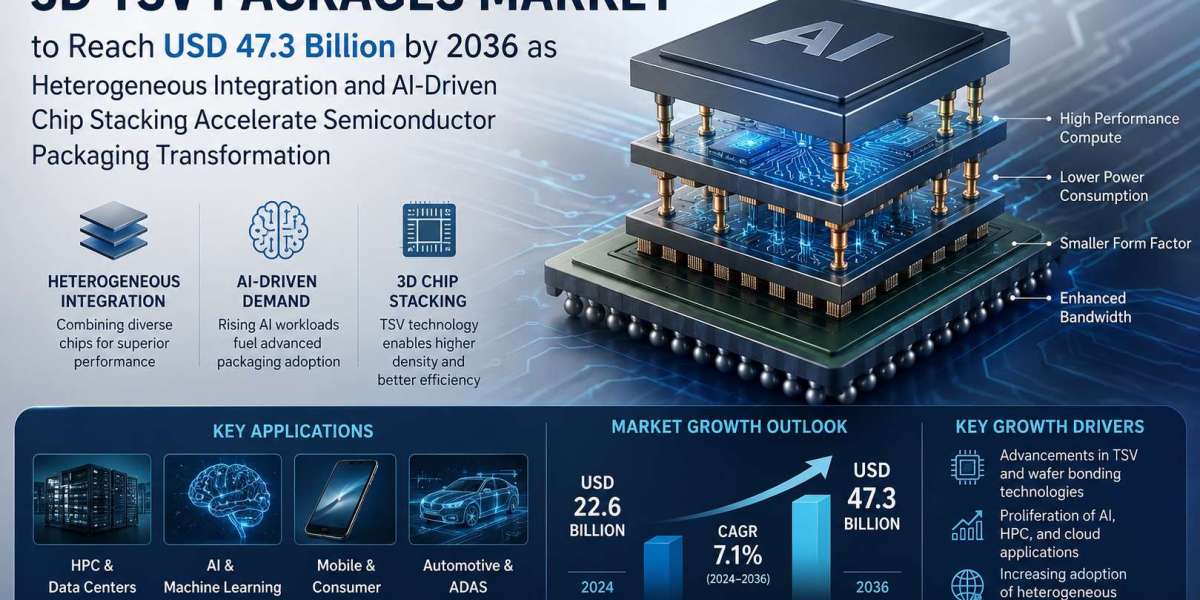
The global 3D TSV packages market is entering a high-growth expansion phase as semiconductor manufacturers accelerate adoption of vertical chip stacking technologies to overcome limitations of traditional planar scaling. According to industry analysis, the market is projected to grow from USD 11.6 billion in 2026 to USD 47.3 billion by 2036, reflecting a CAGR of 15.1%.
Rising demand for high-bandwidth memory (HBM) in AI accelerators, data center processors, and advanced computing systems is significantly increasing the adoption of through-silicon via (TSV) packaging technologies. At the same time, automotive electrification, ADAS systems, and advanced sensor integration are expanding TSV usage beyond traditional consumer electronics applications.
Asia-Pacific continues to dominate production capacity, led by Taiwan, South Korea, and China, while the United States is emerging as a fast-growing hub driven by CHIPS Act investments in advanced semiconductor packaging. Companies with integrated foundry-to-packaging capabilities are gaining strategic advantage in securing long-term supply contracts with hyperscale data center operators.
Get detailed market forecasts, competitive benchmarking, and pricing trends:
https://www.futuremarketinsights.com/reports/3d-tsv-packages-market
Market Overview
The 3D TSV packages market encompasses advanced semiconductor packaging technologies that use through-silicon vias to create vertical electrical connections between stacked dies or interposers. These technologies enable higher interconnect density, reduced latency, and improved thermal performance compared to conventional packaging approaches.
By 2036, the market is expected to reach USD 47.3 billion, up from USD 10.1 billion in 2025. Growth is primarily driven by increasing complexity in semiconductor architectures, particularly in AI and high-performance computing applications requiring heterogeneous integration of logic and memory dies.
Key enabling technologies include via-last, via-first, and via-middle TSV process implementations, which are widely used in wafer-level packaging, chip stacking, and interposer-based integration systems.
Key Growth Drivers
The expansion of the 3D TSV packages market is being fueled by structural changes in semiconductor design and demand patterns.
Key factors include:
Rapid scaling of AI training and inference workloads requiring high-bandwidth memory
• Growth of heterogeneous integration for logic and memory chiplets
• Increasing automotive semiconductor content in EV and ADAS systems
• Expansion of data center infrastructure globally
• Government investments under CHIPS Act and semiconductor sovereignty programs
• Limitations of traditional wire-bond and flip-chip packaging technologies
Among these, AI-driven HBM stacking remains the most significant driver, with TSV-based interconnects enabling data transfer speeds exceeding 1 TB/s in advanced memory systems.
Technology and Innovation Trends
Innovation in 3D TSV packaging is focused on improving interconnect density, thermal performance, and manufacturing efficiency.
Key trends include:
Expansion of via-last process adoption for CMOS-compatible integration
• Advanced wafer thinning and bonding techniques
• Increasing use of copper TSV structures for improved conductivity
• Integration of heterogeneous chiplets in advanced AI processors
• Scaling of HBM3 and next-generation memory architectures
• Development of advanced interposers for multi-die integration
TSV technology is increasingly becoming the backbone of advanced semiconductor packaging used in AI accelerators and high-performance computing platforms.
Market Challenges and Restraints
Despite strong growth momentum, the market faces several structural challenges.
Key restraints include:
High manufacturing costs of TSV formation and wafer processing
• Yield losses associated with die stacking and alignment precision
• Complex thermal management in high-density chip architectures
• Capital-intensive advanced packaging infrastructure
• Limited adoption in cost-sensitive consumer and automotive segments
These challenges restrict TSV adoption primarily to high-performance applications where bandwidth and efficiency gains justify higher costs.
Segment Analysis
Via-Last Process Dominates Market Share
The via-last process realization segment accounts for 46.0% of the market in 2026.
This dominance is driven by its compatibility with standard CMOS fabrication flows and lower integration complexity compared to via-first and via-middle approaches. It enables efficient post-fabrication TSV formation, reducing risk in high-volume production environments.
Other process categories include via-first and via-middle, which are used in specialized applications requiring higher performance or tighter interconnect precision.
Logic and Memory Devices Lead Application Demand
Logic and memory devices represent approximately 58.0% of total application share in 2026.
This segment is driven by:
High-bandwidth memory (HBM2E, HBM3) integration
• AI accelerator and GPU memory stacking
• Heterogeneous integration of processor and memory dies
MEMS, sensors, and power semiconductor applications are also expanding, supported by miniaturization and performance optimization requirements.
Consumer Electronics Remains the Largest End-Use Segment
Consumer electronics account for 43.0% of global demand.
Smartphones, tablets, wearables, and compact computing devices increasingly rely on advanced TSV packaging to achieve high performance within constrained form factors. Automotive, ICT, aerospace, and defense sectors are also contributing steadily to market expansion.
Regional Analysis
United States
The U.S. market is projected to grow at 14.3% CAGR through 2036.
Growth is supported by CHIPS Act investments, strong AI accelerator demand, and expansion of domestic advanced packaging capabilities for defense and data center applications.
China
China is witnessing rapid growth driven by domestic semiconductor self-sufficiency initiatives and expansion of OSAT capabilities for AI and memory packaging.
Japan
Japan benefits from strong semiconductor equipment manufacturing and HBM production expansion supporting TSV adoption.
India
India is emerging as a high-growth market supported by semiconductor incentive programs and electronics manufacturing expansion.
Germany
Germany’s growth is driven by automotive semiconductor demand and European Chips Act investments in advanced packaging infrastructure.
Competitive Landscape
The 3D TSV packages market is highly consolidated, with leading semiconductor companies and OSAT providers dominating global capacity.
The industry is split between:
Vertically integrated semiconductor leaders
• Outsourced packaging and assembly providers
Integrated players are increasingly strengthening control over TSV ecosystems to ensure supply security for AI and high-performance computing applications.
Leading Companies Analysis
Major market participants include:
TSMC
Intel Corporation
Samsung Electronics
ASE Group
Amkor Technology
JCET Group
UMC
SK hynix
Powertech Technology Inc.
Micron Technology
These companies leverage advanced packaging platforms, strong R&D capabilities, and global manufacturing networks to support TSV-based semiconductor production.
Investment and Strategic Developments
Recent developments highlight rapid capacity expansion in advanced packaging:
2025 — TSMC expanded CoWoS advanced packaging capacity to support AI accelerator demand
• 2025 — SK hynix increased HBM production capacity with enhanced TSV-based memory stacking investments
• 2025 — Global OSAT providers announced new facilities targeting AI-driven semiconductor packaging demand
These investments reflect the accelerating shift toward advanced heterogeneous integration in semiconductor manufacturing.
Future Outlook
By 2036, 3D TSV packaging is expected to evolve from a niche advanced packaging solution into a mainstream enabling technology for AI, high-performance computing, and next-generation memory systems.
Future growth will be driven by:
Continued expansion of AI infrastructure
• Scaling of HBM4 and beyond memory technologies
• Increased automotive semiconductor integration
• Advancements in heterogeneous chiplet architectures
• Government-backed semiconductor manufacturing expansion
Asia will remain the dominant production hub, while the United States and Europe will strengthen their focus on advanced packaging innovation and supply chain resilience.
FMI Custom Research: Strategic Intelligence for Confident Decision-Making
In today’s rapidly evolving semiconductor ecosystem, organizations require actionable intelligence tailored to strategic priorities. FMI Custom Research enables decision-makers to evaluate market opportunities, validate investments, and reduce uncertainty in high-capital technology sectors.
Key Executive Benefits:
Decision-ready insights
• Reduced strategic risk
• Market entry validation
• Competitive intelligence advantage
• Faster technology adoption decisions
• Primary industry validation
• Global semiconductor expertise
Business Impact:
FMI helps transform semiconductor market complexity into strategic clarity, enabling faster investment decisions, improved supply chain planning, and stronger competitive positioning.
To explore customized insights:
sales@futuremarketinsights.com
Conclusion
The global 3D TSV packages market is undergoing a structural transformation driven by AI computing demand, heterogeneous integration, and next-generation memory architectures. With market value projected to grow from USD 11.6 billion in 2026 to USD 47.3 billion by 2036, the industry is positioned for sustained high-growth expansion.
As semiconductor scaling approaches physical limits, TSV-based vertical integration is becoming essential for achieving performance improvements. Companies capable of scaling advanced packaging capacity while maintaining yield efficiency and thermal performance will define the future of the semiconductor packaging ecosystem.